


What is Sputtered Deposition?
Sputter deposition is a type of vacuum deposition process that involves the use of a high-energy plasma to “sputter” atoms or molecules from a target material and deposit them onto a substrate. The process takes place in a vacuum chamber, and the target material is typically a solid metal or compound that is placed in a cathode position. The substrate to be coated is placed in an anode position.
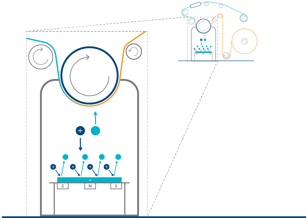
During the sputter deposition process, a high-energy plasma is created by applying an electrical current to the cathode. This plasma ionizes the atoms or molecules in the target material and causes them to be ejected from the surface. The sputtered atoms or molecules travel through the vacuum chamber and are deposited onto the substrate, forming a thin film or coating.
VDI's Sputtering Capabilities
Outlined below are some of the general capabilities of VDI’s sputtering services. For a full list of metals and applications supported please contact us.
Sputter Deposition
Sputter deposition uses a plasma beam to sputter, or knock off, atoms from the source material, which then condense onto the substrate.
Deposition Method
-AC/DC Magnetron Sputtering
-One Single Zone – 3 Targets
-5 Dual, Rotatable Deposition Zones
Substrate Widths
Minimum 40” (1.016 meters) Maximum 74” (1.880 meters)
Thickness Range
0.5 mil – 10 mil
Substrates Supported (Partial)
- Web Polymers including...
- PET
- Nylon
- BOPP
- Fluoropolymers
- Kapton
- Fabrics
- Foils
- Non-wovens
- Synthetic Paper
18 Different Metals Supported including:


Spectrally Selective Component
VDI’s Spectrally Selective component is a highly engineered, multi-layered, film with an optically clear coating that offers superior solar heat rejection, high IR rejection, low visible light rejection and low absorption rate.
Spectrally Selective film provides maximum energy savings with a virtually invisible appearance. VDI’s innovative technology selectively blocks infrared rays while allowing visible sunlight to shine through. Spectrally Selective film is great for maintaining the look of existing glass and is ideal for storefronts, commercial buildings and homes that need minimal light control and excellent heat rejection. The film also reduces passive solar gain even with increased interior illumination levels.
Download the Product SheetWindow Film Component
VDI offers a wide array of component materials that can be used in window film products. From standard metallized aluminum to spectrally selective coatings with different visual appearances and heat rejection properties, VDI can support any window film need. VDI is capable of coating on substrates as thin as 0.5 mil and up to 10 mil.
Download the Product SheetApplications
Sputter deposition is used in a variety of applications, including the production of electronic devices, optics, and decorative coatings. It is a useful technique because it allows for the precise control of the thickness and composition of the deposited film or coating, and it can be used to produce high-quality thin films and coatings. VDI’s capabilities enable it to provide tight tolerances and uniformity of metal deposition, cross web, down-web, and roll-to-roll. In addition, our plasma treatment ensures improved metal adhesion in films.
Industries
Sputter deposition is a method of vacuum deposition that can be employed in a roll-to-roll configuration for scalability and efficiency. Sputter deposition is particularly useful for depositing high-quality, uniform thin films with well-controlled composition and thickness.
In the electronics industry, roll-to-roll sputter deposition plays a significant role in the manufacture of flexible displays and photovoltaic materials for solar panels. The method allows for the deposition of high-quality, uniform films on large-area substrates, which is crucial for achieving the high performance and long-term stability required in these applications.
Additional Industries:
- Electronics and Microelectronics: Manufacturing of flexible circuits, RFID tags, sensors, and more.
- Solar Energy: Production of thin-film solar cells for diverse integrations.
- Display Technology: Creating thin film transistors for flexible displays and OLEDs.
- Packaging: Barrier coatings for product protection.
- Healthcare and Medical Devices: Diagnostic strips, wearable medical device components.
- Automotive: Sensors, flexible displays, and electronic components.
- Aerospace: Coatings and flexible electronics for aircraft and satellites.
- Optics: Anti-reflective coatings, optical filters, and mirrors.
- Battery Technology: Thin film batteries and advanced energy storage.
- Textiles and Wearables: Conductive films and functional coatings for smart textiles.

News & Articles
Latest Blog Posts
What is ITO Sputter Deposition
Indium Oxide/Tin Oxide is among one of the most heavily utilized compounds in the thin film industry due to its electrical conductivity and optical transparency.
Learn more
Vacuum Deposition: A Guide to Thin Film Coating Techniques
One common method for producing thin films is evaporative deposition, which involves the vaporization and subsequent
Learn more
VDI’s Product Development Engineer Receives Technical Award at AIMCAL R2R Conference 2019
Rob Malay, Ph.D., Product Development Engineer at VDI, was the recipient of the John Matteucci Technical Excellence Award at this year’s AIMCAL R2R Conference 2019.
Learn more
VDI Product Development Manager highlights manufacturing advances
Robert Malay, Ph.D., Product Development Manager at VDI, recently co-authored an article for Converting Quarterly entitled “Establishing the flexible-glass R2R coating ecosystem.”
Learn more
VDI Invests in New Equipment, Increases Capacity
VDI today announces a significant investment in new equipment for improved manufacturing with the purchase of a new, world-class vacuum metallizer.
Learn more
Lintec (LUSA) acquires Vacuum Depositing, Inc.
Lintec USA Holding, Inc., a subsidiary of Lintec Corporation, announced today that it has entered into a definitive agreement to acquire Vacuum Depositing, Inc...
Learn more

Ready to Take the Next Step
Ready to explore how VDI's cutting-edge vacuum coating solutions can elevate your products and applications? Contact us today for a free consultation with our experts.
Get a Free Consultation